

![]()
alpha300 Semiconductor Edition - Raman imaging for wafer characterization moves to a bigger stage
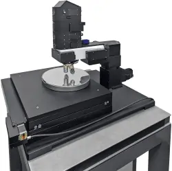 Oxford Instruments WITec has revealed an alpha300 Raman microscope configured especially for semiconductor research and development. It features a large-area scanning stage, wafer chuck options, and an advanced workflow manager to streamline measurements.
Semiconductors are the engines of the information age and the race to understand their properties in ever greater detail is very competitive. The alpha300 Semiconductor Edition consolidates WITec's technological advantages in this field to help researchers accelerate the characterization of chemical composition, crystal quality, strain, and doping in up to 300 mm (12 inch) wafers.
"We started with an alpha300, greatly expanded its scan range, and added software for intuitively defining and sequencing experiments," says WITec Product Manager Thomas Dieing, "This produced an instrument that can examine the biggest wafers with the same precision and convenience as a sample on a microscope slide."
The alpha300 Semiconductor Edition confocal Raman microscope includes active vibration damping, optical profilometer-driven focus stabilization, and comprehensive automation for standardizing measurement procedures and remote operation in controlled environments.
"This is the first of our Focus Editions, a line of pre-configured, application-centered systems that neatly package the benefits we can offer a particular industry," says Harald Fischer, Marketing Director at WITec. "The alpha300 Semiconductor Edition is set up to hit the ground running with groups investigating large semiconductor wafers."
WITec GmbH
Lise-Meitner-Straße 6
D-89081 Ulm
Fon: +49 731 1407 0-0
Fax: +49 731 1407 0-200
Mail: Contact
Web: raman.oxinst.com